LCD and OLED belong to the two camps of displays, which are often discussed in mobile phone display. If you want to figure out what are the main differences between LCD and OLED, let’s move on.
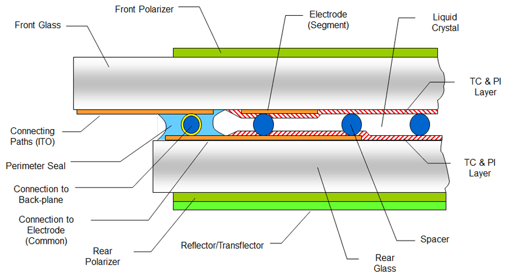
Introduced the basic structure of LCD and the basic principle of LCD display
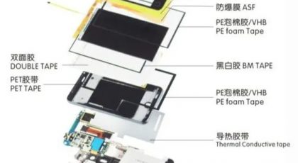
Do you know about the OCA technology? Do you know when do you need to choose OCA? And which kind of OCA material do you need to choose if you are decide go with OCA technology for your touch screen project? Follow Sinocrystal for a detail solution.
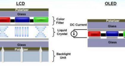
LCD and OLED belong to the two camps of displays, which are often discussed in mobile phone display. If you want to figure out what are the main differences between LCD and OLED, let’s move on.
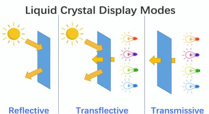
The Difference Between TN, HTN, STN, FSTN LCD Screens
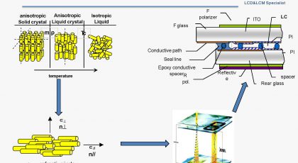
Mono LCD Display Technology Mono LCD technology is actually to pour liquid crystal into two rows of flat surfaces with fine grooves.
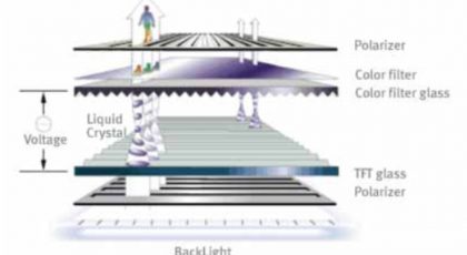
TFT LCD (Thin Film Transistor Liquid Crystal Display) is a thin display type, which has a sandwich-like structure with liquid crystal filled between two glass plates.
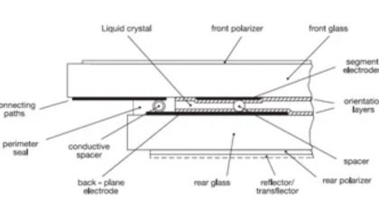
LCD comes from the first letter of liquid crystal display. It’s a passive display component, that means they do not emit light
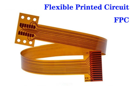
Sinocrystal would like to share with you the technical knowledge of the raw material -- FPC, which to help you understand how to manufacture FPC and the combination of hard and soft board, help us to design the best matching scheme, or provide more angles of analysis ideas in the later anomaly analysis.

Sinocrystal has already shared with you the material of FPC, Now, we would like to share the construction process of FPC with you.

We has discussed the manufacturing steps of Flexible Printed Circuit materials and Flexible Printed Circuit Construction Process. Here we would like to share with you: How to define the areas, layers and stacks of FPC?
The article mainly introduces the TFT-LCD open cell process. The TFT LCD open cell process is generally divided into front, middle and back processes. The front process is mainly for the production of TFT glass; the middle process mainly refers to the pasting of TFT glass and color filters. Bonding; The back-end manufacturing process refers to the pressing of the driver IC, printed circuit board and liquid crystal panel.
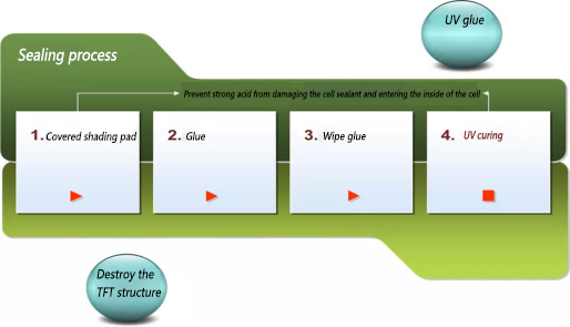
The thinning of the display glass substrate is mainly to use chemical etching and physical polishing to thin the panel module and display glass to meet the needs of light and thin display products. The following panel application requirements can be achieved by thinning the 3.5 inch tft display panel .
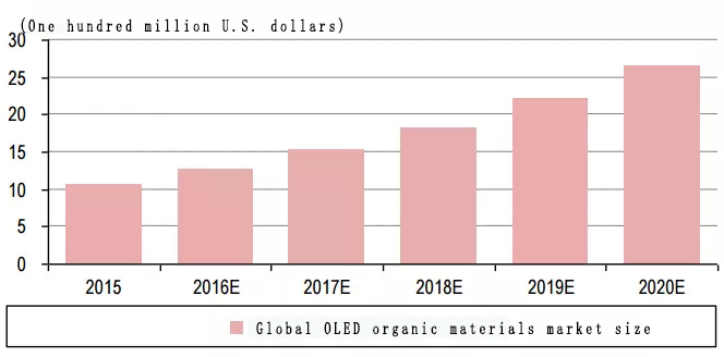
In recent years, OLED has become the focus of industry attention, especially the use of OLED screens in iPhone x smart phones will further promote the industrial application of OLED technology. This article will give a brief description of the materials in OLEDs.
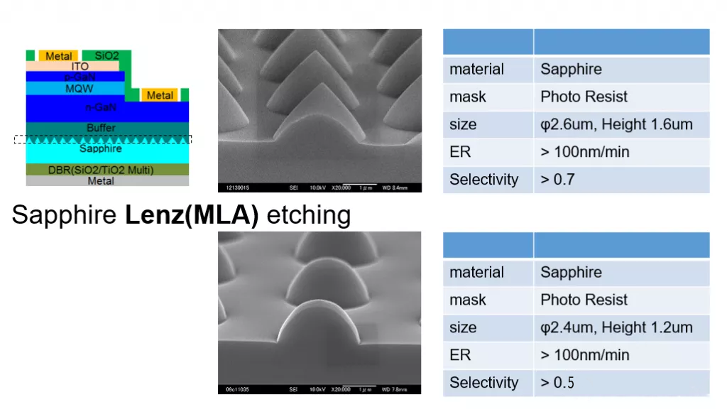
The surface of the substrate is etched to form a cone shape and improve reflectivity. In addition, by forming an AlN Buffer layer, uniform crystal growth and a smooth surface can be achieved.
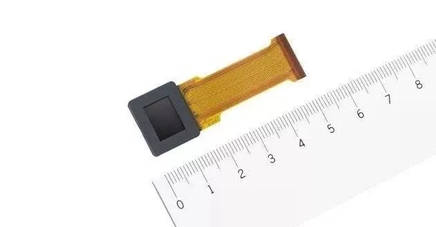
Using a single crystal silicon semiconductor as a substrate, a CMOS driver circuit consisting of ten million transistors is integrated into the semiconductor, and the top layer of the CMOS driver circuit produces an OLED organic light-emitting diode, which is a micro display device that realises both high resolution and tiny size.
OLED strobe is caused by PWM dimming, while LCD is DC dimming. DC dimming is based on the principle of continuous lighting, which improves the screen brightness by increasing or decreasing the power, so changing the voltage or current will improve the screen brightness. Therefore, DC dimming is strobe-free.

Explore the key differences between adhesive-based and adhesive-free FPC substrates—their structures, performance (flexibility, thermal stability, signal integrity), and applications in electronics. Learn why adhesive-free substrates excel in high-frequency, foldable, and automotive systems, while adhesive-based options suit cost-sensitive projects. Optimize your FPC material selection with expert insights.

Selecting the right touch screen for a project is crucial and involves multiple factors. Touch technologies vary: resistive screens are cost - effective and durable with multi - input support, yet have limited resolution and touch accuracy; capacitive screens offer high resolution, sensitivity, and multi - touch but are pricier and non - responsive to non - conductive objects; infrared screens suit large formats and are robust, though less precise. Size depends on project use and space constra

LED backlight is a key component of liquid crystal display, providing light to the screen, so that images and text can be displayed. The paper introduces two main types of backlight: side in and straight down, suitable for thin and light devices and high-end displays respectively. This paper analyzes the principle of backlight, including light guide plate, reflection film, diffusion film and brightening film. With the breakthrough of Mini LED and Micro LED technology, LED backlight technology wi

Learn about LOCA (Liquid Optical Clear Adhesive) full lamination technology, its advantages, and step-by-step process compared to OCA lamination in LCD display bonding.

Learn the key differences between COB (Chip On Board) and COG (Chip On Glass) LCD packaging technologies. Discover which solution best suits your lcd display needs in terms of cost, performance, and application scenarios.

Learn the differences between AG (Anti-Glare), AR (Anti-Reflective), and AF (Anti-Fingerprint) glass surface treatments. Discover how each enhances display performance, visibility, and user experience in various environments.