The surface of the substrate is etched to form a cone shape and improve reflectivity. In addition, by forming an AlN Buffer layer, uniform crystal growth and a smooth surface can be achieved.

The EPI layer is formed by MOCVD and the transparent electric film (ITO) is formed by sputtering.
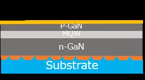
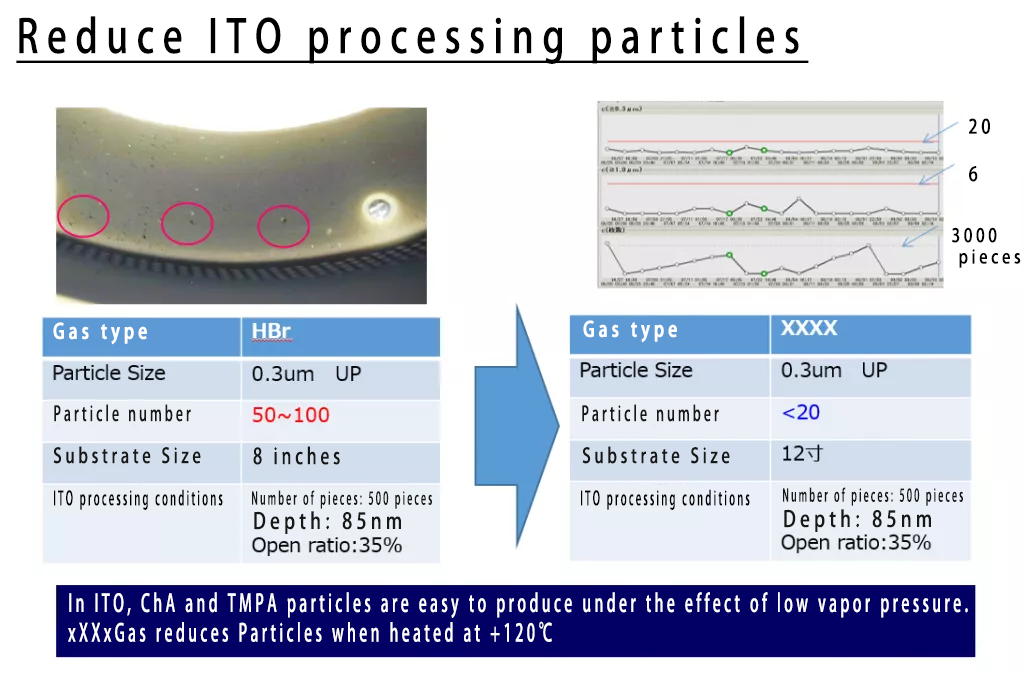
When processing ITO films, particle control is very important.
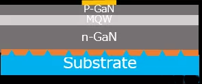

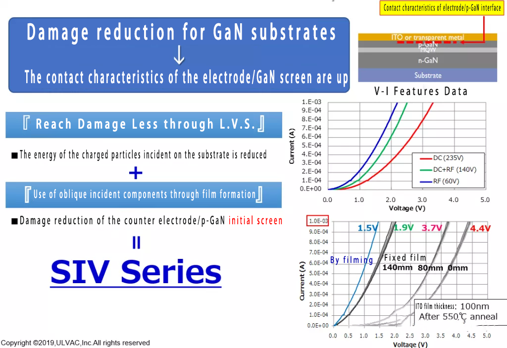
When the ITO film is formed by sputtering, negative ions accelerated in the electric field near the TG surface are incident on the substrate at a high speed, causing damage to the ITO film on the substrate. LVS is a method of lowering the sputtering voltage (negative ion acceleration electric field) and forming an ITO film in a low-damage manner.
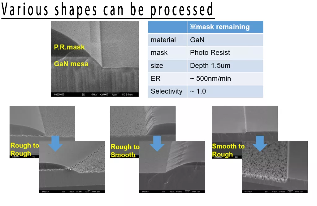
The surface of the substrate is etched to form a cone shape to improve the light reflection efficiency.
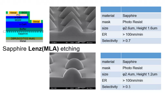
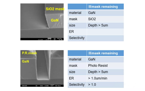
3. Etching (ITO processing)
The 8 inch displays might be affected and delay for an accident.
This is the project management of how sinocrystal handle your customized project relate to displays.
New iPhone 13 Series will use On-Cell OLED Displays. And it that will be launched in the second half of this year will be exclusively supplied by Samsung Display (SDC)
A complete guide to LCD display connection methods, including SPI, I2C, RGB, MIPI, LVDS interfaces and physical mounting options. Learn how to connect monochrome and TFT LCDs to your development board or product housing.
This week, we had the pleasure of hosting an esteemed international client at our LCD display manufacturing facility in Dongguan. Guided by our team, the client visited key production areas such as the fully automated COG bonding line, backlight assembly area, full lamination workshop, and final product aging test section. They highly appreciated our production capacity, strict quality control, and engineering expertise. This visit strengthened mutual trust and set the stage for future collabora
The ILI9881C is a high-performance a-Si TFT LCD single-chip driver developed by ILI Technology Corp. With its excellent display performance and flexible configuration options, this driver meets the modern display device requirements for high resolution and color accuracy. This article will detail the supported resolutions, interfaces, and power supply voltage of the ILI9881C.
The GC9307, a TFT LCD driver with QVGA resolution, has gained widespread use among LCD module manufacturers since its launch. Sinocrystal are excited to share a series of practical insights we have gathered from using the GC9307 driver.